Physics 156 Final: A Brief Survey of FETs
Author:
kdrobers
Last Updated:
12 лет назад
License:
Creative Commons CC BY 4.0
Аннотация:
156 final

\begin
Discover why over 25 million people worldwide trust Overleaf with their work.

\begin
Discover why over 25 million people worldwide trust Overleaf with their work.
\documentclass[11pt]{article}

\usepackage[english]{babel}
\usepackage[utf8]{inputenc}
\usepackage{amsmath}
\usepackage{graphicx}
\usepackage[colorinlistoftodos]{todonotes}

\title{Physics 156 Final: A Brief Survey of FETs}

\author{Kylan Roberson\\kdrobers@ucsc.edu}

\date{\today}

\begin{document}
\maketitle


The thing I found most interesting in our discussions was field effect transistor action. I have previously been exposed to the use of CMOS devices to generate logical switches in computer circuitry, but the explanation for the device mechanics and how they operate was never carefully developed in those classes.

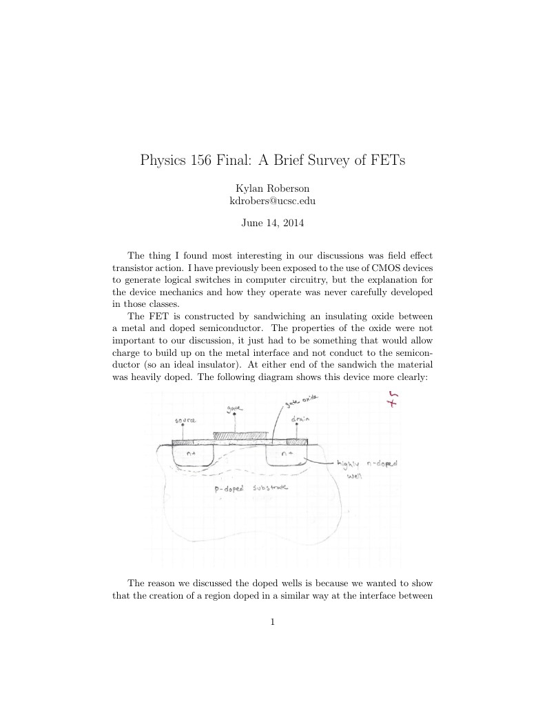
The FET is constructed by sandwiching an insulating oxide between a metal and doped semiconductor. The properties of the oxide were not important to our discussion, it just had to be something that would allow charge to build up on the metal interface and not conduct to the semiconductor (so an ideal insulator). At either end of the sandwich the material was heavily doped. The following diagram shows this device more clearly:

\begin{figure}[!h]
\centering
\includegraphics[width=0.8\textwidth]{nmos.png}
\end{figure}

The reason we discussed the doped wells is because we wanted to show that the creation of a region doped in a similar way at the interface between the semiconductor and oxide would allow the two different wells to conduct between one another.

Next we discussed how we would select a metal such that it’s Fermi energy (the energy needed to excite the electron into a vacuum) would be equal to the chemical potential in the semiconductor at equilibrium similar to the following band diagram with metal on the left and semiconductor on the right:

\begin{figure}[!h]
\centering
\includegraphics[width=0.6\textwidth]{eq.png}
\end{figure}


Note that $\Psi_s$ = $\Psi_m$ in this picture.

Finally we discussed the nature of band bending. When a voltage $V$ is applied to the metal it’s fermi energy drops by $qV$, furthermore, a space charge builds up right at the surface of the metal and creates an E-field that induces charge from the semiconductor towards the oxide interface. This results in the creation of a depletion region in the semiconductor and is shown below:


\begin{figure}[!h]
\centering
\includegraphics[width=0.6\textwidth]{diff.png}
\end{figure}
\pagebreak

If the applied voltage meets a certain threshold, then the bands might bend so that the band furthest from the chemical potential in the equilibrium state is narrowly separated from the chemical potential at the oxide interface. This creates a highly doped region called the inversion layer. The inversion layer allows for heavy majority carrier concentrations to develop at the semiconductor surface and creates a conduction channel between the two doped wells:


\begin{figure}[!h]
\centering
\includegraphics[width=0.6\textwidth]{inv.png}
\end{figure}
\pagebreak

The pictures illustrated here explain a normally off (non conducting in the equilibrium state) NMOS (n-channel conducting) device on p-doped substrate. We also discussed how to adapt this model to oppositely doped devices and metals that had equilibrium fermi energies that were specially chosen to cause enough band bending to induce an inversion layer without the presence of an applied voltage and create a normally on device.

\end{document}